Our Technologies
We are working with modified 5-axis CNC machines for automated precision machining of glass and ceramics at the highest level. We achieve this by combining different machining processes, such as 5-axis CNC coordinate grinding, finishing and polishing on a single machine. This high technology density is complemented by an integrated CAD/CAM chain as well as a high degree of automation, allowing our customers to benefit from a wide range of advantages.
Conventional machining
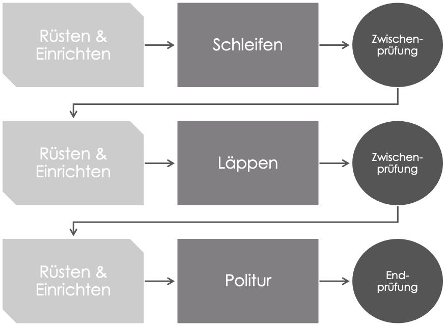
- High machine & tooling costs
- Long setup and inspection times
- Reduced design possibilities of the components
ShapeFab Technology

- Closer tolerances (of components)
- Production times shortened by up to 40%*
- Free component design
*For more details about the ShapeFab Technology please click the following button. You will also get access to our publications.
Technology modules in detail
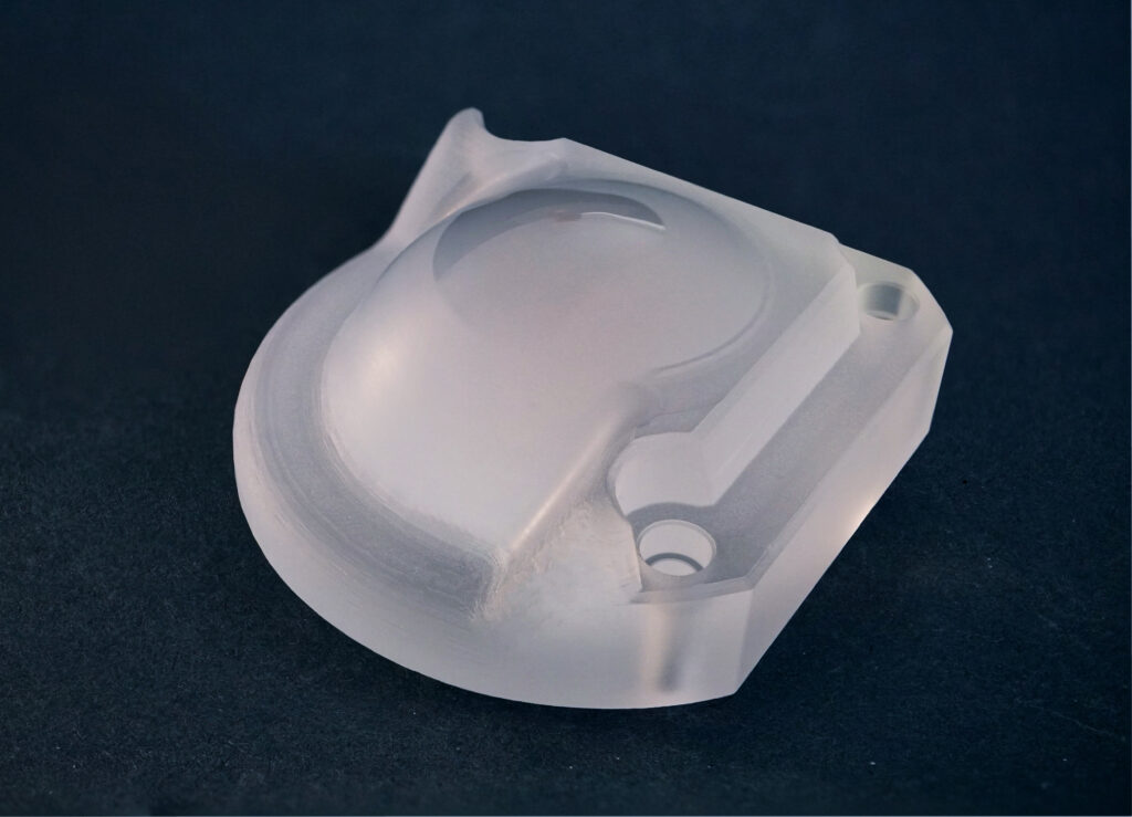
Grinding
Surface roughness Ra = 1200 nm
Finishing
Surface roughness Ra = 200 nm
Polishing
Surface roughness Ra = 8 nm
Figure: Glass free form element
5-axis CNC machining
Coordinate grinding using diamond-bonded tools on high-precision 5-axis CNC machines is used as a core competence. The automated combination of tools with different diamond grit sizes enables optimum process control in terms of surface quality and machining time. Depending on the application, a graded process is used to achieve either high material removal rates or high machining qualities. Currently, transparent and mirror surfaces with roughnesses of up to 8 nm Ra can be applied to any geometry elements using special machining strategies.
CAD/CAM integration
We work with integrated CAD/CAM solutions that have been specially modified by us for glass processing. By using the latest design and manufacturing software, we improve the internal workflow towards a collaborative process. Thus, both design and manufacturing functions can be combined in one model. Digital product development, optimized interfaces to processing machines and measuring devices, and standardized process flows allow development and manufacturing cycles to be significantly shortened. In addition, production costs are reduced and product quality is improved. The processes have a very high reproducibility and automation capability. This enables efficient production of very small batches (batch size 1) and sample parts at series level.
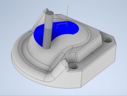
Figure: CAM model of free form element with fixing geometries
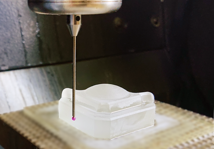
Figure: Measuring process on the machine
In-process measurement
The unmachined parts are measured directly on the CNC machine so that the highest possible manufacturing accuracies can be achieved. In addition, measurements can be made during the machining process via the CAD/CAM system. In this way, for example, dimensional deviations that have occurred due to tool wear can be corrected directly in the process.
Optical and tactile coordinate measuring technology
Through a combination of different sensor systems on one measuring device, almost any contour and component geometries can be measured with an accuracy of a few micrometers. A zoom lens and a chromatic white light sensor also enable visual and non-contact detection of particularly sensitive structures and surface topographies. A flexible probe system is used for efficient tactile measurements. Scanning measurement methods can be used with all sensors, which capture component geometries with a high point density. These generated digital point clouds also allow deviation display against the CAD model.
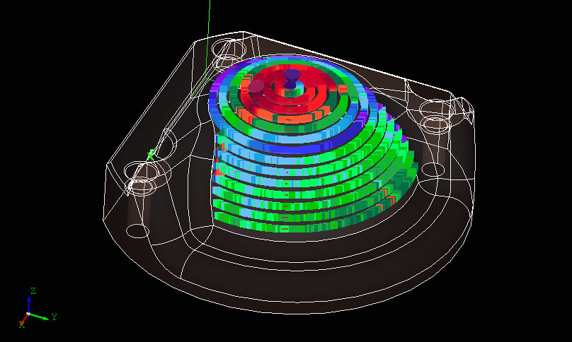
Abbildung: Abweichungsdarstellung auf Basis des CAD-Modells (Werth ScopeCheck)
Figure follows
Precise positioning to existing structures
Mikrooptische Elemente wie Lithographien oder Ätzstrukturen werden kostenoptimiert auf standardisierten Wafern oder Mask Blanks aufgebracht. Mit unserer Technologie können daraus Einzelteile mit dreidimensionalen Geometrien gefertigt werden. Eine exakte Fertigung von Konturen zu diesen Strukturen ist mit Genauigkeiten bis 5 µm möglich.
Highest manufacturing accuracy for your application:
200x200x150 mm
Maximum component sizes
± 3 µm
Manufacturing tolerances
5 µm
Positioning tolerances to existing structures
20 µm
Chipping at component edges
> 300 µm
Min. structures
> 8 nm
Surface roughness (Ra)